
We carry out experimental research in the following areas:
- Materials and devices under high pressures
- Materials under shock compressions
- Nano-photolithography
Materials and Devices under High Pressures
We compress materials, photonic devices and electrochemical systems with GPa (10,000 atm)-level high pressures in a diamond anvil cell to find out-of-box solutions to current major challenges in nano-optics and photonics. High pressure is a powerful tool to systematically tune the intrinsic properties of materials without introducing new chemical component.
Materials of interest include:
- Plasmonic nanomaterials
- Quantum emitters
- Van der Waals (vdW) materials
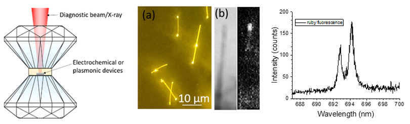
Fig. 1. From left to right: Schematic of compressing electrochemical system and plasmonic devices in a diamond anvil cell; Dark-field image of silver nanowires in a diamond anvil cell; bright-field image and fluorescent image on a silver nanowire; and ruby fluorescence excited at 532 nm.
Materials under Shock Compressions
We also use table-top laser-driven flyer plate apparatus to launch shock waves on bulk and nano-/micro- materials. Shock waves can create irreversible structural and property changes in these materials. The table-top laser-driven flyer plate is a high throughput method that enables the retrieval of shocked samples for post-mortem analysis. Materials of interest include semiconductors, plasmonic materials, and vdW materials. Fig. 2 shows a retrieved semiconductor chip and Raman analysis on the optical phonons before and after shock compressions.
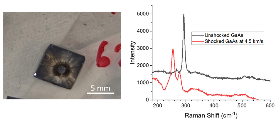
Fig. 2. Raman spectroscopy on shocked and unshocked GaAs chips
Nano-Photolithography
We seek to develop a method for 3D-printing of soft matter with ultra-high resolution. This method overcomes the diffraction limit by surface plasmons and improves the resolution to sub-50 nm by assessing various types of photosensitive resins. Surface plasmons are the collective charge oscillation at metal/dielectric interface. They can be excited by a polarized optical electromagnetic field and are located at the close vicinity of plasmonic structures (e.g. metal nanoparticles) and enhances the local optical field intensity to orders of magnitudes.
We manipulate the optical field at the metal nanoparticle surface, so that the polymerization process was only triggered by surface plasmons. Fig. 3. is an SEM image showing polymer nanostructures were fabricated in the close vicinity of a gold nanodisk.
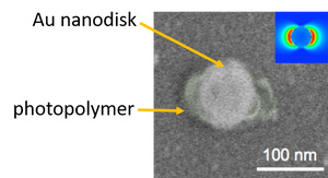
Fig. 3. SEM image on a hybrid structure of metal nanoparticle with photopolymer aligned in one direction. The photopolymer lobes were fabricated with the surface plasmon-triggered photopolymerization with a linearly polarized incident light.
